Ensemble RXTX - Dividers
Band: 30, 20, 17m
Introduction
General Info About the Stage
You might be interested in watching George Thomas' HamNation presentation of building this stage using the heat gun and solder paste method to install the 74AC74 Divider chip (presentation begins at 39:53 into the video).
Theory of Operation
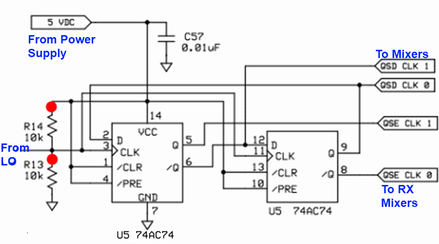
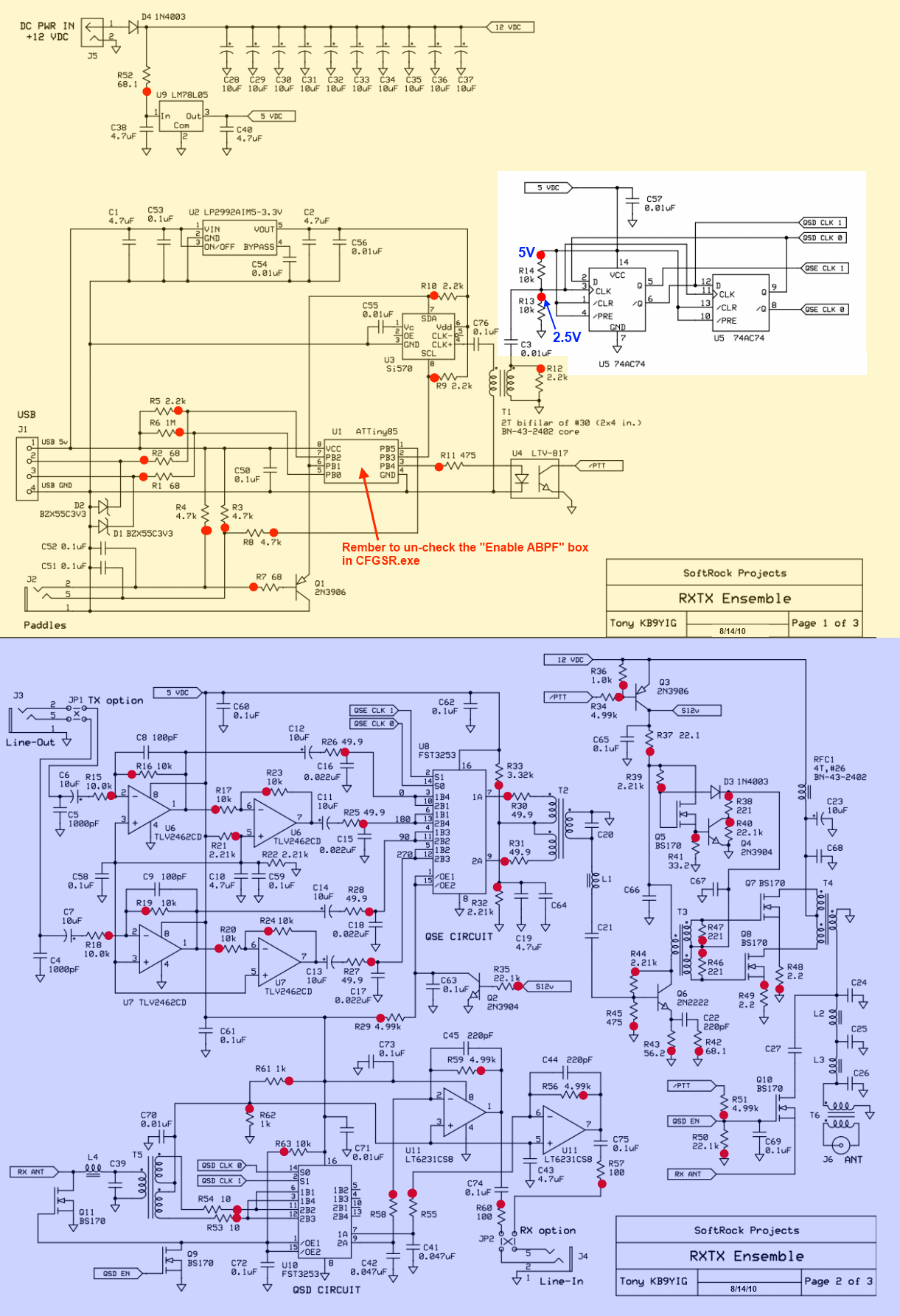
The Dividers stage takes in the local oscillator's signal and divides it by 4, producing two output signals. Each output signal is at a frequency that is ¼ the stage's input signal and is a square wave with 50% duty cycle. The 50% duty cycle is with respect to the regular 5V rail.
The signals are "in quadrature", that is, they are 90° out of phase with each other. These are provided to the TX and RX mixer stages as clocking signals. They are called out on testpoints marked "QSD Clk (1 or 2)", for the I and Q signals to mix down the incoming "chunk" of RF, and "QSE Clk (1 or 2)", for the I and Q signals which mix up the PC's line out signals.
Summary Build Notes
Stage Schematic
Go to Top of Page
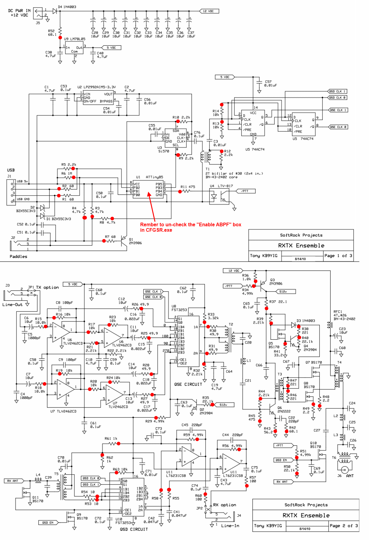
Click here for full schematic
(Red dots represent the "hairpin" (or left-hand or topmost) lead of the component)
Board Layouts
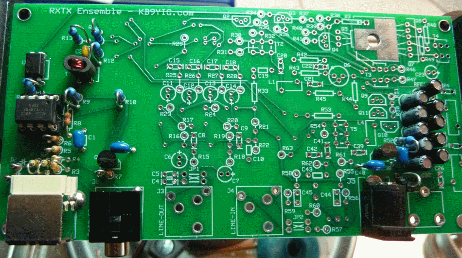
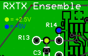
Board Top
Go to Top of Page
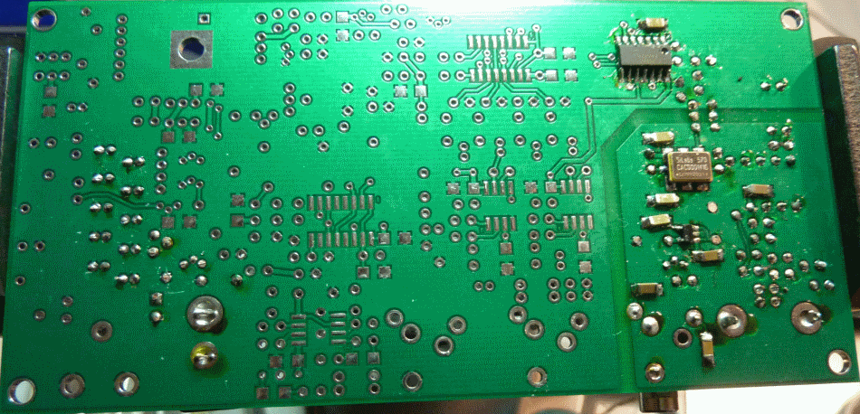
Board Bottom
Go to Top of Page
Dividers Bill of Materials
(30, 20, 17m band option)
(details for installation of each component are provided in the step instructions, further down the page)
| Check | Type | Category | Component | Count | Marking | Image |
|---|---|---|---|---|---|---|
| ☐ | Capacitor | SMT 1206 | 0.01 uF | 1 | (smt) no stripe |

|
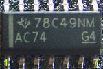
| ☐ | IC | SOIC-14 | 74AC74 Dual D FF | 1 | 74AC74 ESD!!! |
|
| ☐ | Resistor | 1/4W | 10 k 1/4W 1% | 2 | br-blk-blk-r-br |

|
Go to Top of Page
Detailed Build Steps
Step_Install SMT Components
Pay careful attention to the orientation of the divider IC. A number of builders have installed this in the incorrect orientation, resulting in screwy voltages and/or overheated components. You want it installed such that pin 1 is in the upper-right hand corner of the IC when looking at the board as shown in the board graphics. You can see a picture of the orientation of an example divider chip in the BOM for this step.
| Check | Designation | Component (top/bottom) | Orientation | Marking | Image | Band | Notes |
|---|---|---|---|---|---|---|---|
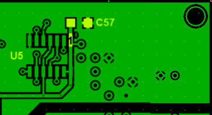
| ☐ | C57 | 0.01 uF ((bottom)) | (smt) no stripe |
|
any | ||
| ☐ | U05 | 74AC74 Dual D FF ((bottom)) | 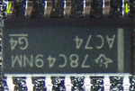 |
74AC74 ESD!!! |
|
any | Markings vary - look for "AC74" |
Go to Top of Page
Step_Install Topside Components
| Check | Designation | Component (top/bottom) | Orientation | Marking | Image | Band | Notes |
|---|---|---|---|---|---|---|---|
| ☐ | R13 | 10 k 1/4W 1% (top) | W-E | br-blk-blk-r-br |
|
any | |
| ☐ | R14 | 10 k 1/4W 1% (top) | S-N | br-blk-blk-r-br |
|
any |
Go to Top of Page
Completed Photos
View of Completed Topside
View of Completed Underside
Go to Top of Page
Progressive Schematic
Where are we in our progress towards the finish line? Click here to view the entire schematic with the completed stages shaded in a yellowish tinge and the remaining stages tinted in blue (the current stage is untinted).
Test the Dividers Stage
Dividers - Current Draw (13V bus)
Power the board on the 13v power jack, connect the USB cable between the PC and the board, and measure the current draw at the power input
Go to Top of Page
Test Steps (if any)
| Step | Test Point | UOM | Nominal | Author's | Builder's |
|---|---|---|---|---|---|
| 0 | Current draw (13V only) | mA | < 20 | 13.2 |
Go to Top of Page
Dividers - Voltage Divider Test
Connect the board to 13V power
Measure following voltages WRT (regular) ground (at R50 hairpin):
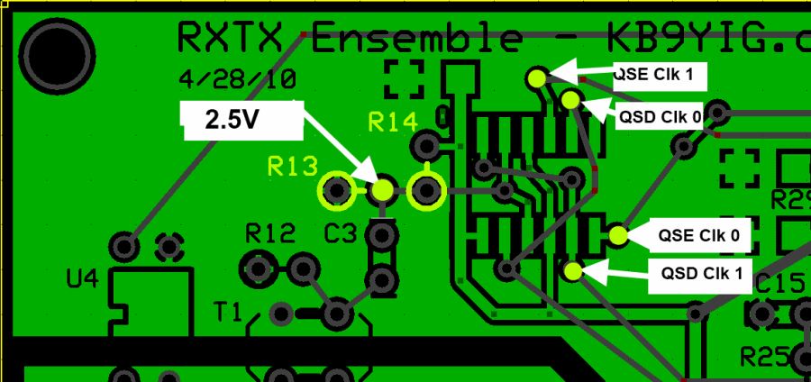
- At the hairpin of R13 (the junction of the R13/R14 voltage divider). You should measure approximately one-half the +5V bus value.
-
At the hairpin of R14. You should measure the 5V rail voltage
Troubleshooting the Voltage Divider
If you do not get the expected R13 value you expect, the possibilities are most likely that you have a short or you have mounted the wrong resistor value(s). For the latter case, you may want to use the utility Voltage Divider Calculator to enter your actual R13 value (Vout and see what resistance values might produce that voltage.
Go to Top of Page
Test Steps (if any)
| Step | Test Point | UOM | Nominal | Author's | Builder's |
|---|---|---|---|---|---|
| 1 | R13 hairpin (wrt regular ground) | Vdc | +2.5 | 2.47 | |
| 2 | R14 hairpin (wrt regular ground) | Vdc | +5 | 4.94 |
Go to Top of Page
Dividers - Divider Output
Plug in the USB cable, power up the Ensemble board, start up CFGSR or the SDR Program, and select a center frequency of 7.040 MHz
Using a frequency measuring device (e.g., freq counter or HF radio), measure the output of the dividers. The frequency should be one -quarter of the local oscillator frequency and should be the center frequency selected in CFGSR or the SDR program.
For example, if the desired center frequency is 7.040 MHz, the putput at each of the four clock outputs should be 7.040MHz (corresponding to a Local Oscillator output of 28.160 MHz.
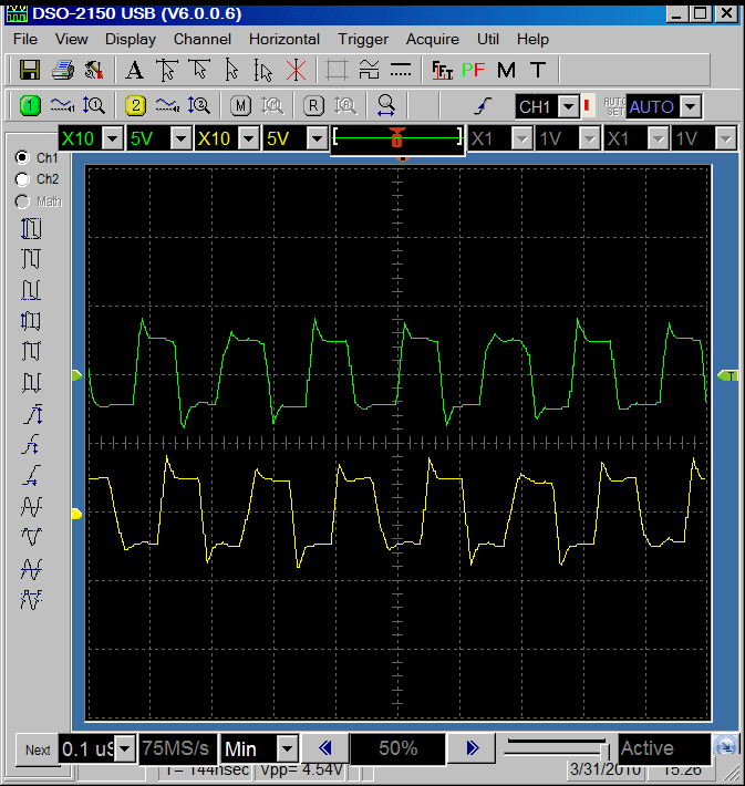
If you have a scope, probe one set of clock outputs (QSE or QSD). You should see two identical waveforms, 90 degrees out of phase with one another.
(the image below is from a USB scope, pushed beyond its meager limits to display the two 7.040 MHz square waves in quadrature!)
Go to Top of Page
Test Steps (if any)
| Step | Test Point | UOM | Nominal | Author's | Builder's |
|---|---|---|---|---|---|
| 0 | QSE Clk 0 | MHz | 7.040 | 7.04 | |
| 1 | QSE Clk 1 | MHz | 7.040 | 7.04 | |
| 2 | QSD Clk 0 | MHz | 7.040 | 7.04 | |
| 3 | QSD Clk 1 | MHz | 7.040 | 7.04 |
Go to Top of Page
Dividers - IC Pin Voltage Tests
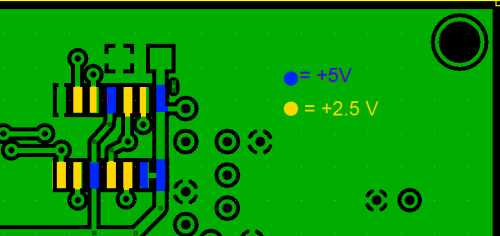
If you do not get results expected in the preceding tests, connect the USB cable, power up the board and measure the pin voltages on U5, per the graphic showing bluie test points for +5 Vdc and yellow test points for 2.5 Vdc.
Keep in mind that there will be some variation on the 2.5V pins, for example pins 11 and 13, which will have some AC component to them from the LO. The critical thing about the voltages on those pins is that they should NOT be zero or 5Vdc. (which would indicate the chip was installed wrong and/or there are bad solder joints/bridges)
These voltages are measured WRT regular ground
Note: the Local Oscillator must be running under USB power AND the dividers must be running under 13V power for the measurements below. If the USB is not connected, measurements will be incorrect.
Go to Top of Page
Test Steps (if any)
| Step | Test Point | UOM | Nominal | Author's | Builder's |
|---|---|---|---|---|---|
| 1 | Pin 1 (blue point) | Vdc | +5 | 4.94 | |
| 2 | Pin 2 (yellow point) | Vdc | +2.5 | 2.45 | |
| 3 | Pin 3 (yellow point) | Vdc | +2.5 | 2.47 | |
| 4 | Pin 4 (blue point) | Vdc | +5 | 4.94 | |
| 5 | Pin 5 (yellow point) | Vdc | +2.5 | 2.44 | |
| 6 | Pin 6 (yellow point) | Vdc | +2.5 | 2.45 | |
| 7 | Pin 7 (regular ground) | Vdc | 0 | 0 | |
| 8 | Pin 8 (yellow point) | Vdc | +2.5 | 2.44 | |
| 9 | Pin9 (yellow point) | Vdc | +2.5 | 2.44 | |
| 10 | Pin 10 (blue point) | Vdc | +5 | 4.94 | |
| 11 | Pin 11 (yellow point) | Vdc | +2.5 | 2.47 | |
| 12 | Pin 12 (yellow point) | Vdc | +2.5 | 2.44 | |
| 13 | Pin 11 (blue point) | Vdc | +5 | 4.94 | |
| 14 | Pin 14 (blue point) | Vdc | +5 | 4.94 |
Go to Top of Page