Ensemble RX III Component Inventory - Combined Kit
Band: (n/a - all parts for all bands are shown)
This page provides a list of components and their maximum quantities to support your inventorying the kit as a whole. This is helpful for kits where the kit includes all parts necessary to build any particular band-specific option (there would, in such cases, likely be excess parts left over at the end of the build).
Once these quantities check out, you can sort the components out to their respective build stages.
| Quantity | Component Type | Category | Component | Photo |
|---|---|---|---|---|
| ☐ 5 | Band-specific | Omit | omit for this band |  |
| ☐ 1 | boardhdw | HDW | 4 X #4-40 hdw (nut, bolt, washer, spacer) | 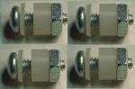 |
| ☐ 2 | Capacitor | Ceramic | 0.015 uF 5%(153) | |
| ☐ 2 | Capacitor | Ceramic | 100 pF 5%(101) | 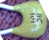 |
| ☐ 2 | Capacitor | Ceramic | 180 pF 5%(181) |  |
| ☐ 1 | Capacitor | Ceramic | 330 pF(331) | 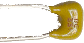 |
| ☐ 2 | Capacitor | Ceramic | 390 pF 5%(391) |  |
| ☐ 3 | Capacitor | Ceramic | 680 pF 5%(681) | 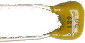 |
| ☐ 2 | Capacitor | Ceramic | 1000 pF 5%(102) |  |
| ☐ 2 | Capacitor | Ceramic | 1500 pF 10%(152) | 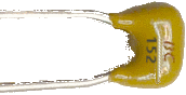 |
| ☐ 2 | Capacitor | Ceramic | 1800 pF 5%(182) | |
| ☐ 3 | Capacitor | Ceramic | 3300 pF 5% |  |
| ☐ 3 | Capacitor | Ceramic | 6800 pF 5%(682) | |
| ☐ 1 | Capacitor | Ceramic | 0.01 uF(103) |  |
| ☐ 2 | Capacitor | Ceramic | 0.047 uF 5%(473) |  |
| ☐ 5 | Capacitor | Ceramic | 4.7 uF 10% 16V X7R RAD |  |
| ☐ 20 | Capacitor | SMT 1206 | 0.1 uF |  |
| ☐ 1 | connector | Jack | BNC Connector Male - PCB mount |  |
| ☐ 1 | Connector | Jack-RA | 3.5mm stereo jack - PCB mount (rt-angle) |  |
| ☐ 1 | Connector | Jack-RA | DC Power Jack PCB Mount (rt-angle) 2.5mm |  |
| ☐ 1 | connector | Jack-RA | USB-B pcb jack (rt-angle) |  |
| ☐ 1 | Connector | Plug | DC Power Plug 5.5/2.5mm Pos Ctr |  |
| ☐ 1 | Diode | Axial | 1N4003 | 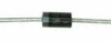 |
| ☐ 2 | Diode | Axial | BZX55C3V3 3.3V zener diode |  |
| ☐ 1 | IC | DIP 8 | ATtiny 85-20 PU w/V15.12 Firmware | 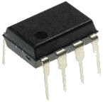 |
| ☐ 2 | IC | DIP-4 | LTV-817 Opto-Isolator |  |
| ☐ 1 | IC | I2C | Si570 Programmable Oscillator | 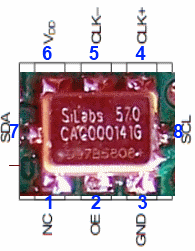 |
| ☐ 1 | IC | SOIC-14 | 74AC74 Dual D FF | 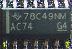 |
| ☐ 3 | IC | SOIC-16 | FST3253 mux/demux switch |  |
| ☐ 1 | IC | SOIC-8 | LT6231 dual op-amp |  |
| ☐ 1 | IC | SOT-23-5 | LP2992AIM5-3.3V regulator |  |
| ☐ 1 | IC | TO-92 | LM78L05 voltage regulator |  |
| ☐ 3 | inductor | Binocular core | BN-43-2402 (no markings!)(none) |  |
| ☐ 1 | Inductor | coil | 0.13uH: 7T #30 on T25-6 core |  |
| ☐ 2 | Inductor | coil | 0.46uH: 13T #30 on T25-6 core | |
| ☐ 1 | Inductor | coil | 0.46uH: 10T #30(8in) on T30-2(red)(red) | |
| ☐ 2 | Inductor | coil | 1uH: 19T #30(9in) on T25-6(yel)(yellow) | |
| ☐ 1 | Inductor | coil | 1.3uH: 17T #30(11in) on T30-2(red)(red) | |
| ☐ 2 | inductor | Coil | 2uH: 21T #30(13in) on T30-2(red)(red) | |
| ☐ 1 | Inductor | coil | 2.6uH: 24T #30(15in) on T30-2(red)(red) | |
| ☐ 1 | Inductor | coil | 2.7uH: 25T #30(15in) on T30-2(red)(red) | |
| ☐ 3 | Inductor | coil | 4.6uH: 32T #30(18in) on T30-2(red)(red) | |
| ☐ 2 | Inductor | coil | 5.5uH: 35T #30(20in) on T30-2(red)(red) | |
| ☐ 2 | Inductor | coil | 10uH: 48T #30(26in) on T30-2(red)(red) | |
| ☐ 2 | Inductor | coil | 20uH: 68T #30(36in) on T30-2(red)(red) | |
| ☐ 1 | Inductor | coil | 26uH: 80T #30(43in) on T37-2(red)(red) | |
| ☐ 1 | Inductor | coil | 0.27uH: 10T #30 on T25-6 c(yellow) | |
| ☐ 2 | Inductor | coil | 55uH: 117T #30(61in) on T37-2(red)(red) | |
| ☐ 6 | inductor | Toroid | T25-6 toroid core(yellow) |  |
| ☐ 9 | inductor | Toroid | T30-2 toroid core(red) |  |
| ☐ 3 | inductor | Toroid | T37-2 toroid core(red) | |
| ☐ 1 | Inductor | xfrmr | 5.76uH: 2T(bi)T #30(5 (2x2.5)in) on BN43-2402 | |
| ☐ 1 | Inductor | xfrmr | 12.96uH: 3T(bi)T #30(10 (2x5)in) on BN43-2402 | |
| ☐ 1 | Inductor | xfrmr | 23.04uH: 4T(bi)T #30(8 (2x4)in) on BN43-2402 | |
| ☐ 1 | Inductor | xfrmr | 23.04uH: 4T/2T(bi)T #30(9(4/2x2.5)in) on BN43-2402 | |
| ☐ 1 | Inductor | xfrmr | 70.56uH: 7T(bi)T #30(16 (2x8)in) on BN43-2402 | |
| ☐ 1 | Inductor | xfrmr | 70.56uH: 7T/3T(bi)T #30(18 (8/2x5)in) on BN43-2402 | |
| ☐ 1 | PCB | Main Board | Ensemble RX PCB (board) | |
| ☐ 2 | Resistor | 1/4W | 10 ohm 1/4W 1%(br-blk-blk-gld-br) |  |
| ☐ 2 | Resistor | 1/4W | 49.9 ohm 1%(yel-wht-wht-gld-brn) |  |
| ☐ 2 | Resistor | 1/4W | 4.99 k 1/4W 1%(y-w-w-br-br) |  |
| ☐ 3 | Resistor | 1/6W | 68 1/6W 5%(bl-gry-blk-gld) |  |
| ☐ 4 | Resistor | 1/6W | 75 1/6W 5%(vio-grn-blk-gld) |  |
| ☐ 2 | Resistor | 1/6W | 120 1/6W 5%(brn-red-brn-gld) |  |
| ☐ 12 | Resistor | 1/6W | 2.2k 1/6W 5%(red-red-red-gld) |  |
| ☐ 5 | Resistor | 1/6W | 10 k 1/6W 5%(brn-blk-ora-gld) |  |
| ☐ 1 | Resistor | 1/6W | 1 M 1/6W 5%(brn-blk-grn-gld) |  |
| ☐ 1 | Resistor | User-Supplied | 10 k Test Resistor | |
| ☐ 1 | socket | Socket | 8 pin dip socket | |
| ☐ 4 | wire | Cutoff | shunt wire (cut-off lead) | |
| ☐ 6 | wire | Magnetic | Magnetic Wire, enameled #30 | |