Softrock_40_R Operational Amplifiers
Band: 20m
Introduction
General Info About the Stage
Theory of Operation
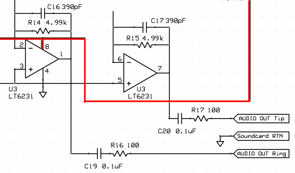
This stage implements a pair of high-gain operational amplifiers to amplify and low-pass filter the I and Q outputs of the mixers, delivering "audio-level" signals from 0 to ~100 kHz to the "ring" and "tip" terminals for input to the stereo line-in inputs of the (PC's) sound card.
Stage Schematic
Go to Top of Page
Board Layouts
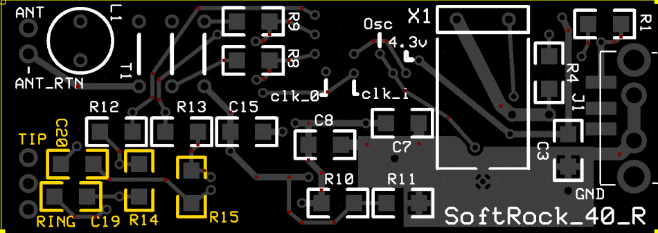
Board Top
Go to Top of Page
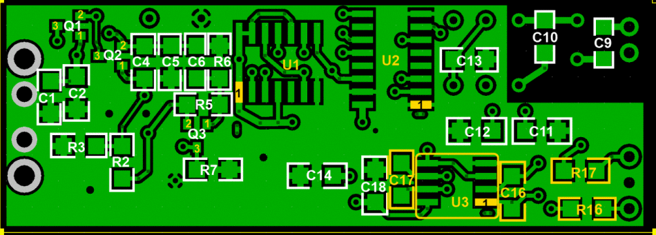
Board Bottom
Go to Top of Page
Operational Amplifiers Bill of Materials
( 20m band option)
(details for installation of each component are provided in the step instructions, further down the page)
| Check | Type | Category | Component | Count | Marking | Image |
|---|---|---|---|---|---|---|
| ☐ | Capacitor | SMT 1206 | 390pF 5% | 2 | in bag |

|
| ☐ | Capacitor | SMT 1206 | 0.1 uF | 2 | (smt) black stripe |

|
| ☐ | IC | SOIC-8 | LT6231 dual op-amp | 1 | LT6231 ESD!!! |

|
| ☐ | Resistor | SMT 1206 1/4W | 100 1/4W 5% | 2 | 101 |

|
| ☐ | Resistor | SMT 1206 1/4W | 4.99k 1/4W 1% | 2 | 4991 |

|
Go to Top of Page
Detailed Build Steps
Install Underside Components
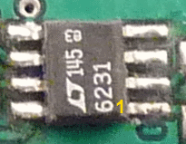
C16 and C17 will install very close to U3. Take care in installing them to be sure there are no solder splashovers to adjacent pins of U3. C16 connects to pins 1 and 2 of U3; C17 connects to pins 7 and 6 of U3. See the graphic:
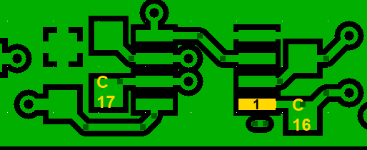
U3 Orientation
| Check | Designation | Component | top/Bottom | Marking | Image | Band | |
|---|---|---|---|---|---|---|---|
| ☐ | C16 | 390pF 5% ((bottom)) | in bag |
 |
20m | ||
| ☐ | C17 | 390pF 5% ((bottom)) | in bag |
 |
20m | ||
| ☐ | R16 | 100 1/4W 5% ((bottom)) | 101 |
 |
any | ||
| ☐ | R17 | 100 1/4W 5% ((bottom)) | 101 |
 |
any | ||
| ☐ | U03 | LT6231 dual op-amp ((bottom)) | LT6231 ESD!!! |
 |
any |
Install Topside Components
| Check | Designation | Component | top/Bottom | Marking | Image | Band | |
|---|---|---|---|---|---|---|---|
| ☐ | R14 | 4.99k 1/4W 1% (top) | 4991 |
 |
20m | ||
| ☐ | R15 | 4.99k 1/4W 1% (top) | 4991 |
 |
20m | ||
| ☐ | C19 | 0.1 uF (top) | (smt) black stripe |
 |
any | ||
| ☐ | C20 | 0.1 uF (top) | (smt) black stripe |
 |
any |
Completed Photos
Note: the completed pictures are of the 20m option, which the author built. Other band options (which the author did not build) will appear slightly different (especially the inductors, whose windings and cores will vary by band) for the band-specific components.
View of Completed Topside

View of Completed Underside

Go to Top of Page
Testing
Overview
Before doing any testing, use a bright light and good magnification to verify correct soldering. Soldering problems are the greatest cause of test failures. Pay particular attention to U3.
USB Rail Integrity Test
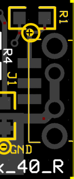
Before powering up, check the resistance across the 5V USB connections (pins 1 (5V) and 4 (gnd) of J1). If you get something very close to zero, you may have introduced a short and the possibility of "frying" your PC's USB Power Bus.
Voltage Tests - U3 Pins
When measuring pin voltages on U3, test the voltage on BOTH the pin and the pad. This will drive out any cases where the pad has the requisite voltage, but a bad solder joint causes the pin not to have the same voltage.
Test Table
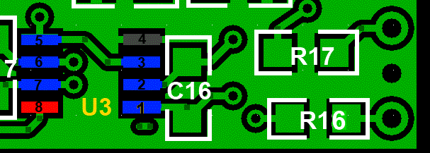
Apply USB power and measure the voltages at the following test points/pin numbers shown in the figure below:
| Seq | Test Point | Units | Nominal Value |
Author's Value | Your Value |
|---|---|---|---|---|---|
| 1 ☐ | U3 - Pin 1 | Vdc | 2.15 | 2.09* | ___________ |
| 2 ☐ | U3 - Pin 2 | Vdc | 2.15 | 2.06 | ___________ |
| 3 ☐ | U3 - Pin 3 | Vdc | 2.15 | 2.06 | ___________ |
| 4 ☐ | U3 - Pin 4 | Vdc | 0 | 0 | ___________ |
| 5 ☐ | U3 - Pin 5 | Vdc | 2.15 | 2.06 | ___________ |
| 6 ☐ | U3 - Pin 6 | Vdc | 2.15 | 2.06 | ___________ |
| 7 ☐ | U3 - Pin 7 | Vdc | 2.15 | 2.09* | ___________ |
| 8 ☐ | U3 - Pin 8 | Vdc | 4.3 | 4.13 | ___________ |
* pins 1 and 7 are the amplified I and Q outputs. They have been known to show different pin voltages from the other nominally 2.15V pins.